

-
 Redaction
Why copper still rules the motherboard trace
Copper still dominates motherboard traces. See how conductivity, skin effect, and dielectric loss together shape PCIe 6.0 and DDR5 signal integrity today.
The fundamental physics of copper in modern computing
In the hierarchy of materials science, copper occupies a specific niche that has made it indispensable to the electronics industry for decades. When evaluating the architecture of a high-speed motherboard, the choice of conductor material is not merely a matter of historical tradition but a calculated engineering decision based on atomic-level performance. Copper serves as the primary conduit for both data and power, balanced against the strict constraints of cost, manufacturability, and durability.
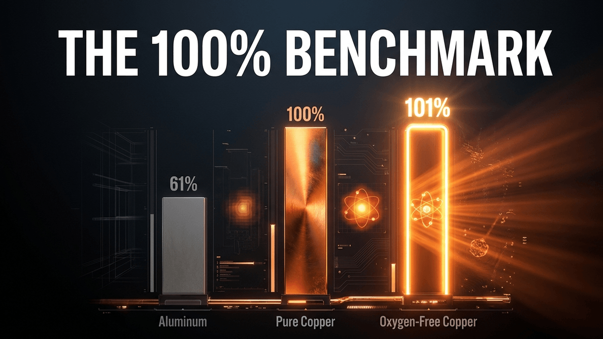
Electrical conductivity is the most critical metric for any PCB trace. Copper is second only to silver in its ability to conduct electricity among all metals. Pure copper is used as the baseline with a 100% conductivity rating; however, specialized variants like oxygen-free copper can actually reach 101% conductivity relative to that benchmark. This efficiency is a direct result of copper's atomic structure. Its valence electrons move with minimal resistance, allowing for a high current density without the excessive resistive heating that plagues other metals.
For example, aluminum offers only 61% of the conductivity of copper, which would necessitate significantly larger traces to carry the same electrical load. In the dense environment of a modern ATX or server motherboard, where space is at a premium, copper's superior conductivity allows engineers to shrink trace widths while maintaining the necessary current carrying capacity.
Low resistivity and the maintenance of signal strength
Resistivity is the inverse of conductivity, and in high-speed applications, low resistivity is the primary defense against signal degradation. As electrical signals travel down a motherboard trace, they inevitably lose energy due to the resistance of the metal itself. This phenomenon, known as conductor loss, becomes more pronounced as traces get longer or signals reach higher frequencies. By utilizing copper, designers can minimize DC resistance, which helps maintain the voltage amplitude of a signal as it moves from a CPU to a distant memory module or PCIe slot.
To combat ohmic losses in high-performance designs, engineers often specify thicker copper layers. While a standard consumer-grade PCB might use 1 oz of copper per square foot, high-speed or high-power designs frequently utilize 2 oz or 3 oz layers. This increased thickness reduces the total resistance of the trace, which is particularly vital for long buses that must maintain strict signal-to-noise ratios. Recent hardware teardowns show 3 oz copper becoming increasingly common in high-end workstations, ensuring that PCB signal loss does not interfere with the tight tolerances required by modern data transfer protocols.
There's a wrinkle here worth flagging, though, because it isn't universally true across every high-speed interface. On the newest PCIe generations, thicker isn't automatically better - and I'll come back to why once we get to the loss budgets these boards actually have to hit.
Precision impedance control in high-frequency environments
The transition from simple electrical signals to high-speed data transmission introduces the concept of characteristic impedance. At frequencies used by DDR5 memory or Gen 5 and Gen 6 PCIe lanes, a PCB trace acts as a transmission line rather than a simple wire. Maintaining a consistent impedance is essential to prevent signal reflections. If a signal encounters a change in impedance, a portion of its energy reflects back toward the source, causing data errors, jitter, and destructive interference.
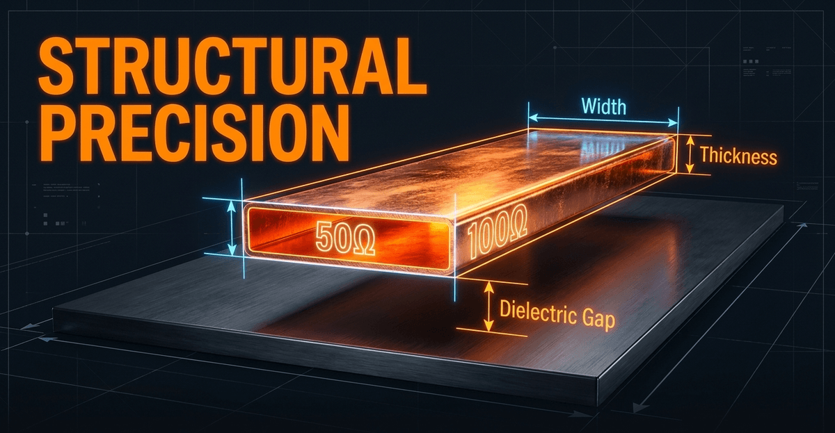
Copper's role in impedance control is structural. The characteristic impedance of a trace is determined by its width, the thickness of the copper foil, and the distance to the reference ground plane. Because copper can be plated and etched with extreme precision, manufacturers can maintain highly uniform trace dimensions. This level of control allows for the creation of matched-impedance pairs where the tolerance is often measured in single-digit percentages.
Modern DDR5 designs illustrate just how unforgiving this has become. Holding a consistent 50-ohm single-ended impedance across an entire signal path now demands manufacturing tolerances tighter than plus or minus 10 percent, and differential pair lengths typically need to be matched within about two mils of each other to avoid skew-induced reflections. Without the predictable physical properties of copper, achieving the 50-ohm or 100-ohm standards required for high-speed differential signaling would be practically impossible at scale.
What happens when impedance is wrong
A typical DDR5 server motherboard packs in kilometers of copper trace once you add up every signal, power, and ground path across a 12- to 16-layer stack - and a single mismatched differential pair, off by just a few mils, is enough to unravel the signal integrity budget for an entire memory channel. That gap between the scale of the problem and the tolerance for error is what makes impedance control the part of motherboard engineering where theory meets the factory floor most directly.
In practice, an engineer chasing an impedance-wrong trace starts with a Time-Domain Reflectometer (TDR). The TDR sends a fast edge down the trace and reads back the reflections, plotting impedance as a function of distance along the signal path. A clean 50-ohm trace shows up as a flat line; a via, a sudden width change, or a spot where the trace strays too close to a plane edge shows up as a visible bump or dip. Where that bump appears on the plot tells the engineer exactly where the physical defect sits on the board.
The consequences of ignoring that bump scale with frequency. A 5% impedance mismatch on a DDR4 bus might shave a few percent off the eye diagram margin - a nuisance, not a failure. The same 5% mismatch on a DDR5 or PCIe 6.0 lane, where the eye is already a third narrower thanks to PAM4 signaling, can be the difference between a link that trains reliably and one that fails intermittently under load - the kind of fault that passes every bench test and then reappears at a customer's site under real thermal and electrical stress. That's why impedance debugging on a modern board increasingly happens before fabrication, not after: designers run 2D field-solver simulations on every critical trace geometry, cross-check against the stack-up's actual copper thickness and dielectric height, and only release the design to manufacturing once the simulated impedance sits inside the required window. Post-fabrication TDR testing on a small sample of the first production run then confirms that what got etched matches what got simulated - a discrepancy at that stage usually means the copper thickness or etch process drifted from spec, not that the original design was wrong.
Thermal management through copper density
Beyond its role as a signal carrier, copper functions as the central nervous system for thermal management on a motherboard. Silicon components like VRMs (Voltage Regulator Modules) and high-performance chipsets generate significant thermal energy that must be moved away from the die to prevent throttling or failure. Copper excels as a thermal conductor, with a thermal conductivity that is roughly 58% higher than that of aluminum. It heats and cools rapidly, allowing it to act as an efficient conduit for thermal energy.
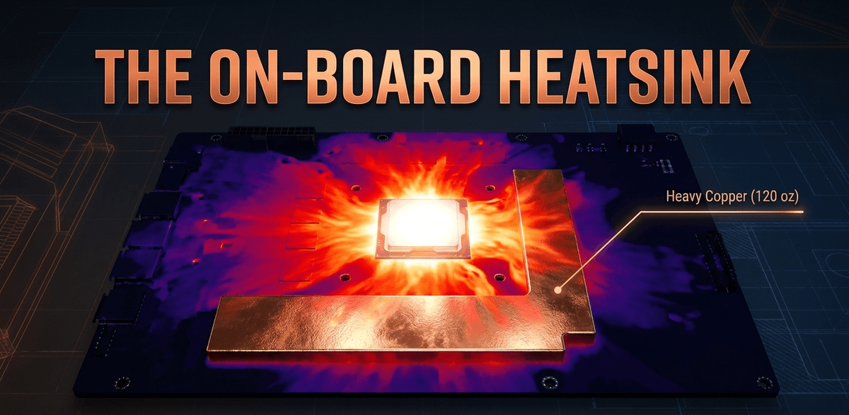
Engineers utilize copper pours - filling unused areas of the PCB with solid copper - to create internal heat sinks. These copper planes spread heat horizontally across the board, increasing the effective surface area for cooling. In specialized power-delivery boards, "heavy copper" techniques are employed. These designs use copper weights ranging from 4 oz to as high as 20 oz. In extreme cases, copper plating up to 120 oz can be integrated directly into the board, serving as an on-board heatsink that eliminates the need for bulky external metal plates.
A well-designed copper plane does two jobs at once: it moves heat away from the die, and it gives high-speed signals the clean, low-inductance return path they need to stay quiet.
This horizontal and vertical integration of thermal management into the PCB structure itself is a primary reason copper remains the dominant material for power-dense electronics. It's worth noting that DDR5 modules alone now consume 20 to 30 percent more power than their DDR4 equivalents at comparable data rates, which puts even more pressure on the copper pours surrounding the memory subsystem to keep temperatures in check.
High-frequency challenges: the skin effect
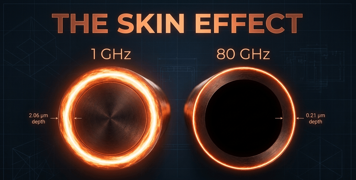
As signal frequencies climb into the gigahertz range, a phenomenon known as the skin effect begins to complicate the use of copper. At low frequencies, current flows through the entire cross-section of a trace. However, as frequency increases, the magnetic fields generated by the current push the electrons toward the outer edges of the conductor. This results in the current flowing only through a thin "skin" of the copper, effectively reducing the conductive area and increasing AC resistance.
Technical data shows that at 1 GHz, copper's skin depth is approximately 2.06 micrometers. By the time a signal reaches 80 GHz, the skin depth shrinks to a mere 0.21 micrometers. This reduction in effective area leads to significant signal attenuation. Engineers must account for this by either adjusting trace geometry or using specialized copper treatments to compensate for the lost signal amplitude. The skin effect is a physical limit that forces a move toward more sophisticated copper handling rather than a move away from copper itself.
Here's where the earlier point about copper thickness resolves itself. On PCIe 6.0 boards, engineers don't simply pile on more copper to fight loss - excessive copper thickness actually increases insertion loss at these frequencies once the skin effect confines current to a thin outer layer. High-speed PCIe 6.0 plating tends to stay at 1 oz or thinner, paired with a very smooth copper foil, rather than following the "go thicker" logic that works for lower-frequency power buses. Thickness solves a DC resistance problem; smoothness and geometry solve a gigahertz problem, and the two goals pull in different directions.
The impact of copper surface roughness on insertion loss
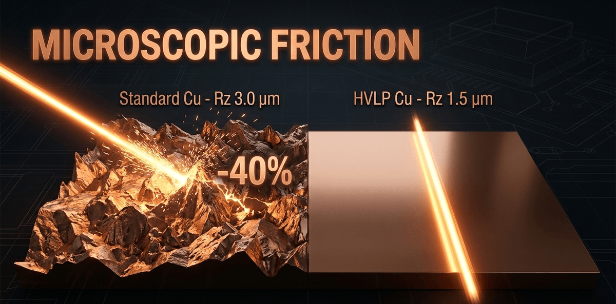
In high-speed PCB design, the microscopic finish of the copper foil is just as important as its purity. To improve the bond between the copper foil and the resin of the dielectric layer, manufacturers often use copper with a roughened surface. While this roughness is beneficial for mechanical adhesion, it is detrimental to high-frequency signals. Because the skin effect forces current to the surface, the electrons must travel along the peaks and valleys of the copper's texture, effectively increasing the path length and the resistance.
Research indicates that surface roughness can increase the effective resistance of a transmission line by up to 40% at frequencies exceeding 1 GHz. A practical example of this is seen in the reduction of Rz values (a measure of roughness height). Reducing the Rz from 3.0 μm to 1.5 μm can lower insertion loss by approximately 0.1 dB per inch at 10 GHz. To address this, chip manufacturers and board designers now specify Very Low Profile (VLP) or Hyper Very Low Profile (HVLP) copper foils. These materials are nearly as smooth as a mirror on the microscopic level, ensuring that signal loss is kept to an absolute minimum in high-bandwidth applications.
PCIe 6.0 pushes this requirement even further down the stack. Because the specification's PAM4 signaling scheme has almost no margin left to absorb loss, HVLP-grade copper foil - or better - has effectively become table stakes rather than a premium option for any board that intends to run Gen 6 lanes at full length.
Dielectric properties and the signal environment
While copper provides the path, the insulating material (dielectric) surrounding the copper determines how fast and how cleanly the signal moves. Two key metrics define this relationship: the Dielectric Constant (Dk) and the Dissipation Factor (Df). The Dk measures how much the material slows down the electromagnetic wave. High-speed PCBs require materials with a low and stable Dk, typically between 2.2 and 3.5 for frequencies above 1 GHz, to ensure fast signal propagation and to maintain consistent impedance.
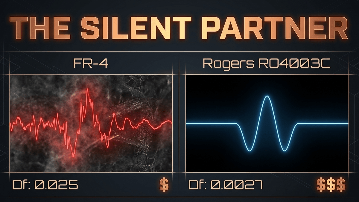
Conversely, the Dissipation Factor (Df), or loss tangent, quantifies how much signal energy is lost as heat due to the dielectric material absorbing the energy of the oscillating electromagnetic field. Standard FR-4 material, which is ubiquitous in low-cost electronics, has a Df between 0.018 and 0.025. This is far too high for modern high-speed designs. In contrast, specialized laminates like Rogers RO4003C feature an ultra-low Df of 0.0027 at 10 GHz.
The choice of dielectric is essentially a choice of how much the designer is willing to pay to protect the signal integrity provided by the copper traces. High-speed designs often use a hybrid approach, using specialized laminates for critical signal layers while relying on cheaper FR-4 for power and ground planes.
What PCIe 6.0 and DDR5 demand from the copper layer
It's worth pausing here to put hard numbers on how much tighter the loss budget has become, because this is where copper's limitations, rather than its strengths, drive the engineering conversation.
PCIe 6.0 moves to PAM4 signaling, packing two bits into each unit interval instead of one. That gets you a doubling of throughput to 64 GT/s without doubling the frequency, but it comes at a cost: PAM4's four voltage levels shrink the vertical eye diagram opening by roughly a third compared to the two-level NRZ scheme used in earlier PCIe generations. With less voltage margin to work with, the specification has to be brutally strict about how much loss the channel is allowed to introduce.
The numbers tell the story plainly:
- At 64 Gbps with a 32 GHz Nyquist frequency running in NRZ mode, differential insertion loss would hit roughly -58 dB - a loss so severe that no realistic equalizer could recover an acceptable bit error rate.
- Switching to PAM4 keeps the effective Nyquist frequency at 16 GHz, the same as PCIe 5.0, which is the only reason the channel loss stays manageable at all.
- Even so, PCIe 6.0's total channel loss budget is capped at roughly 32 dB, and the PCB portion of that budget is generally held to about 13.5 dB maximum.
- To keep a trace at the conventional 13.5-inch length under that budget, the board material has to hold PCB loss to around 1.00 dB per inch - a target that pushes designers toward Megtron 6 or Megtron 7-class laminates well before Gen 6 becomes mainstream.
DDR5 tells a related but distinct story. Because it introduced on-die error correction, a dual 32-bit channel architecture, and decision feedback equalization, a typical DDR5 server motherboard now needs 12 to 16 layers, compared with 8 to 12 for an equivalent DDR4 board. Achieving the target 40-ohm single-ended impedance with practical trace widths of 3.5 to 5 mils generally requires dielectric thicknesses of 3.0 to 4.5 mils between the signal and reference layers, which in turn pushes many designs into HDI-class fabrication. Via stubs become resonant antennas at these frequencies too, so boards thicker than 1.6 mm typically need back-drilling to keep stub length under 10 mils, or blind and buried microvias to eliminate the stub problem outright.
Both standards arrive at the same underlying lesson from different directions: copper hasn't stopped being the right conductor, but the margin for error in how that copper is shaped, plated, and paired with dielectric material has essentially disappeared.

Manufacturing pragmatism and cost efficiency
Despite the rising costs of raw materials, copper remains the most cost-effective solution when performance is taken into account. While raw copper can be up to three times more expensive than aluminum, the manufacturing ecosystem is entirely built around copper processing. The chemistry of etching, plating, and soldering is optimized for copper. Attempting to use a different material would require a total overhaul of the global supply chain, likely offsetting any potential material savings.
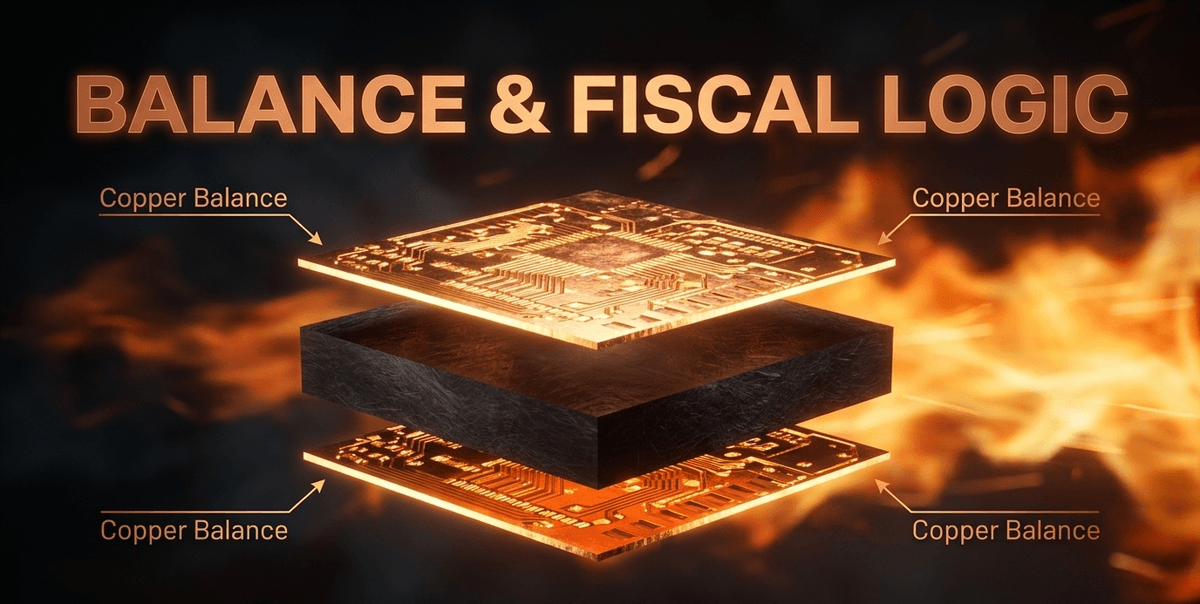
Furthermore, copper's role in the manufacturing process itself contributes to board reliability. Maintaining a copper balance - ensuring that the density of copper is relatively uniform across different layers of a multilayer PCB - is vital. If one side of a board has significantly more copper than the other, the different rates of thermal expansion will cause the board to warp or delaminate during the high-heat soldering process. By using copper pours and carefully distributed ground planes, manufacturers produce flatter, more reliable boards that are less likely to fail during assembly or in the field.
Industry reporting also suggests that major server OEMs have needed six to twelve months of yield learning when moving motherboard designs from DDR4 to DDR5, largely due to how demanding the new signal integrity tolerances are on the manufacturing floor. That's a useful reminder that copper's cost advantage isn't just about the raw metal - it's about decades of accumulated process knowledge that newer materials simply don't have yet.
Advanced copper configurations for power and grounding
The use of copper pour and ground planes is not just for thermal management; it is a fundamental tool for Electromagnetic Interference (EMI) suppression. By covering unused areas with copper, designers create stable reference planes. These planes provide the shortest possible return path for signals, which reduces the size of the current loops and minimizes the emission of electromagnetic noise. Without these copper-rich environments, modern PCs would likely interfere with every wireless device in their vicinity.
Heavy copper PCBs take this further by providing extreme current-carrying capacity in a compact form factor. While a 3 oz copper PCB can increase total board costs by 30-50% compared to a standard 1 oz design, the reliability gains are immense. In high-power applications like electric vehicle controllers or industrial power supplies, the enhanced mechanical strength and heat dissipation of heavy copper prevent catastrophic failures that would be far more expensive than the initial material cost.
For readers who want to see how these same signal integrity principles carry over into memory subsystem design specifically, it's worth reading up on how DDR5 routing and layer stacking has evolved to meet these tighter tolerances - the copper pour strategy on a modern memory subsystem and the strategy on a PCIe channel are solving closely related problems with slightly different constraints.
This economic reality ensures that even as alternative materials are explored, copper's combination of physics and fiscal logic remains unchallenged.
Could anything actually replace copper?
It's a fair question, and the honest engineering answer is: not yet, and not for the traces that matter most.

Graphene is the material most often cited as copper's eventual successor. Its electron mobility exceeds copper's, and its thermal conductivity is excellent, which has made it attractive for flexible electronics and transparent conductive films. Silver has slightly better raw conductivity than copper too, and silver-plated copper is already used in applications where marginal conductivity gains justify the added expense. Researchers have also made real progress on graphene-based hole metallization as a lower-pollution alternative to electroless copper plating in specific manufacturing steps, and on laser-induced graphene scaffolds that seed copper deposition for flexible circuit boards.
None of this amounts to graphene or silver displacing copper on a rigid, high-speed motherboard, though. Silver's scarcity and cost make it impractical at the volumes a motherboard requires. Graphene, for all its promise, remains difficult to integrate at scale into the etching and lamination processes that copper fabrication has spent decades refining. What's actually happening in current PCB manufacturing is more modest and more pragmatic: copper stays as the trace material, while alternative substances substitute in around it - immersion silver or electroless nickel immersion gold as surface finishes, for instance, rather than as replacements for the copper trace itself.
The more realistic trajectory, at least through the PCIe 6.0 and DDR5 era, is refinement rather than replacement: smoother foils, lower-loss dielectrics, and smarter equalization electronics doing the work that a fundamentally different conductor might otherwise have to do.
Future projections and specialized laminates
As we look toward future standards beyond PCIe 6.0, the role of copper will continue to evolve through refined material science rather than replacement. The industry is moving toward even smoother foils and more advanced dielectric pairings. Materials like Megtron 6, Megtron 7, and Rogers RO4350B are becoming standard in high-end networking and server environments because they offer the low Dk and Df values required to support data rates that were previously unimaginable.
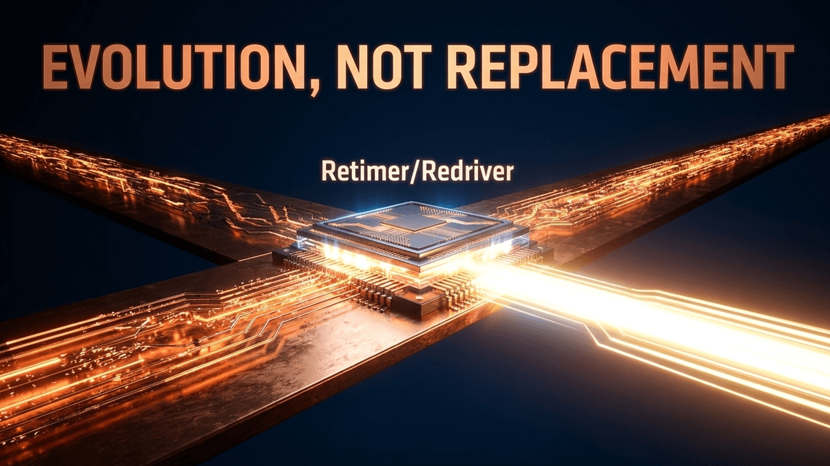
In the long term, the engineering focus will likely remain on mitigating the limitations of copper at high frequencies. This involves the use of signal conditioning chips like redrivers and retimers that boost signal strength and clean up jitter, allowing copper traces to stretch a bit further than physics would normally allow - PCIe 6.0 designs, for instance, generally require ultra-low-loss materials or an added retimer for any trace longer than about 10 inches. Until a material comes along that offers significantly better conductivity than copper at a comparable price and with similar ease of manufacturing, copper will remain the foundation of the digital world.
Its unique balance of electrical, thermal, and mechanical properties makes it the only viable choice for the high-speed traces that power our modern infrastructure. Every CPU breakthrough, every faster SSD, every new GPU still depends on electrons traveling through copper that engineers continue refining rather than replacing.
Share now









Key takeaways
- Copper is second only to silver in electrical conductivity among all metals; oxygen-free copper can reach 101% of the standard IACS conductivity rating.
- Aluminum offers only 61% of copper's conductivity, which is why it can't simply replace copper without much larger trace geometry.
- Copper's thermal conductivity is roughly 58% higher than aluminum's, making it central to heat dissipation on power-dense boards.
- High-speed and high-power designs commonly use 2 oz to 3 oz copper layers, while "heavy copper" boards range from 4 oz up to 120 oz for on-board heatsinking.
- At 1 GHz, copper's skin depth is about 2.06 micrometers; at 80 GHz, it shrinks to just 0.21 micrometers, concentrating current in a thinner conductive layer.
- Copper surface roughness can raise effective transmission line resistance by up to 40% at frequencies above 1 GHz.
- Reducing copper foil roughness (Rz) from 3.0 μm to 1.5 μm can lower insertion loss by about 0.1 dB per inch at 10 GHz.
- PCIe 6.0's PAM4 signaling caps total channel loss near 32 dB, with the PCB portion generally limited to about 13.5 dB.
- Unlike lower-frequency buses, PCIe 6.0 designs favor thinner (≈1 oz), smoother copper foil, since excess thickness increases insertion loss at gigahertz frequencies.
- A typical DDR5 server motherboard requires 12 to 16 PCB layers, versus 8 to 12 for equivalent DDR4 designs.
- Low-loss dielectrics like Rogers RO4003C achieve a Dissipation Factor of just 0.0027 at 10 GHz, versus 0.018-0.025 for standard FR-4.
- A 3 oz copper PCB can raise total board costs by 30-50% over a standard 1 oz design, but prevents far costlier failures in high-power applications.
Sources
- Altium (DDR5 PCB layout and signal integrity guidelines) https://resources.altium.com/p/ddr5-pcb-design-and-signal-integrity-what-designers-need-to-know
- Cadence (PCIe 6.0 electrical testing white paper) https://www.cadence.com/content/dam/cadence-www/global/en_US/documents/tools/silicon-solutions/design-ip/pcie-6-0-electrical-testing-for-high-data-bandwidth-applications.pdf
- Altium (how copper foil roughness affects signals and impedance) https://resources.altium.com/p/how-copper-foil-roughness-affects-your-signals-and-impedance
- Epectec (heavy copper PCB design) https://www.epectec.com/articles/heavy-copper-pcb-design.html
- Prysmian Group (why use copper as an electrical conductor) https://uk.prysmian.com/media/news/why-use-copper-as-an-electrical-conductor
- Published 2026-07-23 08:28
- Modified 2026-07-23 08:28

-
Redaction